
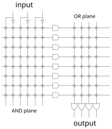
A programmable logic array (PLA) is a kind of programmable logic device used to implement combinational logic circuits. The PLA has a set of programmable AND gate planes, which link to a set of programmable OR gate planes, which can then be conditionally complemented to produce an output. It has 2N AND gates for N input variables, and for M outputs from the PLA, there should be M OR gates, each with programmable inputs from all of the AND gates. This layout allows for many logic functions to be synthesized in the sum of products canonical forms.
PLAs differ from programmable array logic devices (PALs and GALs) in that both the AND and OR gate planes are programmable. PAL has programmable AND gates but fixed OR gates[clarification needed]
YouTube Encyclopedic
-
1/5Views:1 016 46330 491591 99732 87412 458
-
Programmable Logic Array (PLA) | Easy Explanation
-
Digital Logic - Programmable Logic Arrays
-
Programmable Array Logic (PAL)
-
Lecture 1: Programmable Logic Array Part 1
-
Digital Logic - Programmable Array Logic
Transcription
History
In 1970, Texas Instruments developed a mask-programmable IC based on the IBM read-only associative memory or ROAM. This device, the TMS2000, was programmed by altering the metal layer during the production of the IC. The TMS2000 had up to 17 inputs and 18 outputs with 8 JK flip-flops for memory. TI coined the term Programmable Logic Array for this device.[1]
Implementation procedure
- Preparation in SOP (sum of products) form.
- Obtain the minimum SOP form to reduce the number of product terms to a minimum.
- Decide the input connection of the AND matrix for generating the required product term.
- Then decide the input connections of the OR matrix to generate the sum terms.
- Decide the connections of the inversion matrix.
- Program the PLA.
PLA block diagram:
| 1ST BLOCK | 2ND BLOCK | 3RD BLOCK | 4TH BLOCK | 5TH BLOCK |
|---|---|---|---|---|
| INPUT BUFFER | AND MATRIX | OR MATRIX | INVERT/ NON INVERT MATRIX | FLIP-FLOP OUTPUT BUFFER |
Advantages over read-only memory
The desired outputs for each combination of inputs could be programmed into a read-only memory, with the inputs being driven by the address bus and the outputs being read out as data. However, that would require a separate memory location for every possible combination of inputs, including combinations that are never supposed to occur, and also duplicating data for "don't care" conditions (for example, logic like "if input A is 1, then, as far as output X is concerned, we don't care what input B is": in a ROM this would have to be written out twice, once for each possible value of B, and as more "don't care" inputs are added, the duplication grows exponentially); therefore, a programmable logic array can often implement a piece of logic using fewer transistors than the equivalent in read-only memory. This is particularly valuable when it is part of a processing chip where transistors are scarce (for example, the original 6502 chip contained a PLA to direct various operations of the processor[2]).
Applications
One application of a PLA is to implement the control over a datapath. It defines various states in an instruction set, and produces the next state (by conditional branching). [e.g. if the machine is in state 2, and will go to state 4 if the instruction contains an immediate field; then the PLA should define the actions of the control in state 2, will set the next state to be 4 if the instruction contains an immediate field, and will define the actions of the control in state 4]. Programmable logic arrays should correspond to a state diagram for the system.
The earliest Commodore 64 home computers released in 1982 (into early 1983) initially used a programmed Signetics 82S100 PLA, but as the demand increased, MOS Technology / Commodore Semiconductor Group began producing a mask-programmed PLA, which bore part number 906114-01.[3]
See also
References
- ^ Andres, Kent (October 1970). A Texas Instruments Application Report: MOS programmable logic arrays. Texas Instruments. Bulletin CA-158.
- ^ How MOS 6502 Illegal Opcodes really work
- ^ arcadecomponents.com - Commodore 906114-01 64 PLA IC
External links
- "Programmable Logic Array (PLA)". cmsc311. University of Maryland. 2003. Archived from the original on 2017-12-14.
- "PLA (programmable logic array)". Java Applet. University of Hamburg. Archived from the original on 2013-01-15. Retrieved 2010-04-07.
| Authority control databases: National |
|---|