

A multi-chip module (MCM) is generically an electronic assembly (such as a package with a number of conductor terminals or "pins") where multiple integrated circuits (ICs or "chips"), semiconductor dies and/or other discrete components are integrated, usually onto a unifying substrate, so that in use it can be treated as if it were a larger IC.[1] Other terms for MCM packaging include "heterogeneous integration" or "hybrid integrated circuit".[2] The advantage of using MCM packaging is it allows a manufacturer to use multiple components for modularity and/or to improve yields over a conventional monolithic IC approach.
A Flip Chip Multi-Chip Module (FCMCM) is a multi-chip module that uses flip chip technology. A FCMCM may have one large die and several smaller dies all on the same module.[3]
YouTube Encyclopedic
-
1/4Views:7 5321 337136 2234 857
-
Mod-03 Lec-14 Multichip modules (MCM)-types; System-in-package (SIP); Packaging roadmaps
-
DVD - Lecture 10d: System-in-Package (SiP)
-
A Brief History of Semiconductor Packaging
-
Hybrid Or Multi Chip ICS(Integrated Circuit)(हिन्दी)
Transcription
Overview
Multi-chip modules come in a variety of forms depending on the complexity and development philosophies of their designers. These can range from using pre-packaged ICs on a small printed circuit board (PCB) meant to mimic the package footprint of an existing chip package to fully custom chip packages integrating many chip dies on a high density interconnection (HDI) substrate. The final assembled MCM substrate may be done in one of the following ways:
- The substrate is a multi-layer laminated printed circuit board (PCB), such as those used in AMD's Zen 2 processors.
- The substrate is built on ceramic, such as low temperature co-fired ceramic
- The ICs are deposited on the base substrate using Thin Film technology.
The ICs that make up the MCM package may be:
- ICs that can perform most, if not all of the functions of a component of a computer, such as the CPU. Examples of this include implementations of IBM's POWER5 and Intel's Core 2 Quad. Multiple copies of the same IC are used to build the final product. In the case of POWER5, multiple POWER5 processors and their associated off-die L3 cache are used to build the final package. With the Core 2 Quad, effectively two Core 2 Duo dies were packaged together.
- ICs that perform only some of the functions, or "Intellectual Property Blocks" ("IP Blocks"), of a component in a computer. These are known as chiplets.[4][5] An example of this are the processing ICs and I/O IC of AMD's Zen 2-based processors.
An interposer connects the ICs. This is often either organic (a laminated circuit board that contains carbon, hence organic) or is made of silicon (as in High Bandwidth Memory).[6] Each has advantages and limitations. Using interposers to connect several ICs instead of connecting several monolithic ICs in separate packages reduces the power needed to transmit signals between ICs, increases the number of transmission channels, and reduces delays caused by resistance and capacitance (RC delays).[7] However, communication between chiplets consumes more power and has higher latency than components within monolithic ICs.[8]
Chip stack MCMs
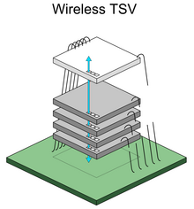
A relatively new development in MCM technology is the so-called "chip-stack" package.[9] Certain ICs, memories in particular, have very similar or identical pinouts when used multiple times within systems. A carefully designed substrate can allow these dies to be stacked in a vertical configuration making the resultant MCM's footprint much smaller (albeit at the cost of a thicker or taller chip). Since area is more often at a premium in miniature electronics designs, the chip-stack is an attractive option in many applications such as cell phones and personal digital assistants (PDAs). With the use of a 3D integrated circuit and a thinning process, as many as ten dies can be stacked to create a high capacity SD memory card.[10] This technique can also be used for High Bandwidth Memory.
The possible way to increasing the performance of data transfer in the Chip stack is use Wireless Networks on Chip (WiNoC).[11]
Examples of multi-chip packages
- IBM Bubble memory MCMs (1970s)
- IBM 3081 mainframe's thermal conduction module (1980s)
- Superconducting Multichip modules (1990s)[12][13]
- Intel Pentium Pro, Pentium II OverDrive, Pentium D Presler, Xeon Dempsey, Clovertown, Harpertown and Tigerton, Core 2 Quad (Kentsfield, Penryn-QC and Yorkfield), Clarkdale, Arrandale, Kaby Lake-G, and models with Crystalwell (those with the GT3e or GT4e graphics)
- SD cards, Micro-SD cards and Sony memory sticks
- eMMC and eUFS
- Xenos, a GPU designed by ATI Technologies for the Xbox 360, with eDRAM
- POWER2, POWER4, POWER5, POWER7, POWER8, and Power10 from IBM
- IBM z196
- Nintendo's Wii U Espresso (microprocessor) has its CPU, GPU, and onboard VRAM (integrated into the GPU) on one MCM.[14]
- VIA Nano QuadCore[15]
- Flash and RAM memory combined on a PoP by Micron
- Samsung MCP solutions combining mobile DRAM and NAND storage.[16][17][18]
- AMD Ryzen Threadripper and Epyc CPUs based on Zen or Zen+ architecture are MCMs of two or four chips[19] (Ryzen based on Zen or Zen+ is not MCM and consist of one chip)
- AMD's non-APU Ryzen, Ryzen Threadripper and Epyc CPUs based on the Zen 2 or Zen 3 architecture are MCMs of one, two, four[20] or eight chips containing CPU cores and one bigger I/O chip[21]
- AMD Instinct MI series GPUs based on CDNA 2 architecture are MCMs of one or two graphics compute die (GCD) chips.
- AMD Radeon RX 7000 series GPUs based on RDNA 3 architecture are MCMs with one GCD and up to six memory cache die (MCD) chips.
- Intel Xe Ponte Vecchio GPUs
- Intel Meteor Lake CPUs
- Any other processor with High Bandwidth Memory
- Apple M series with CPU and memory
3D multi-chip modules
See also
- System in package (SIP)
- System on a chip (SoC)
- Hybrid integrated circuit
- Advanced packaging (semiconductors)
- Chip carrier Chip packaging and package types list
- Single Chip Module (SCM)
- UFS Multi Chip Package (uMCP)
References
- ^ Rao Tummala, Solid State Technology. "SoC vs. MCM vs SiP vs. SoP", Retrieved August 4, 2015.
- ^ Don Scansen, EE Times "Chiplets: A Short History Retrieved 26 April, 2021
- ^ "IMAPS Advancing Microelectronics 2020 Issue 3 (Advanced SiP)". FlippingBook. Retrieved 2023-12-05.
- ^ Samuel K. Moore, IEEE Spectrum "Intel's View of the Chiplet Revolution" Retrieved 26 April, 2021
- ^ Semi Engineering "Chiplets" Retrieved 26 April, 2021
- ^ "2.5D - Semiconductor Engineering". Semiengineering.com. Retrieved 2022-05-13.
- ^ "Interposers".
- ^ Dr. Ian Cutress, AnandTech "Intel Moving to Chiplets: 'Client 2.0' for 7nm"
- ^ Jon Worrel (15 April 2012). "Intel migrates to desktop Multi-Chip Modules (MCMs) with 14nm Broadwell". Fudzilla.
- ^ Richard Chirgwin, The Register. “Memory vendors pile on '3D' stacking standard.” April 2, 2013. February 5, 2016.
- ^ Slyusar V. I., Slyusar D.V. Pyramidal design of nanoantennas array. // VIII International Conference on Antenna Theory and Techniques (ICATT’11). - Kyiv, Ukraine. - National Technical University of Ukraine “Kyiv Polytechnic Institute”. - September 20–23, 2011. - Pp. 140 - 142. [1]
- ^ Ghoshal, U.; Van Duzer, T. (1992). "High-performance MCM interconnection circuits and fluxoelectronics". Proceedings 1992 IEEE Multi-Chip Module Conference MCMC-92. pp. 175–178. doi:10.1109/MCMC.1992.201478. ISBN 0-8186-2725-5. S2CID 109329843.
- ^ Burns, M. J.; Char, K.; Cole, B. F.; Ruby, W. S.; Sachtjen, S. A. (1993). "Multichip module using multilayer YBa2Cu3O7−δinterconnects". Applied Physics Letters. 62 (12): 1435–1437. Bibcode:1993ApPhL..62.1435B. doi:10.1063/1.108652.
- ^ Satoru Iwata, Iwata Asks. “Changes in Television.” Retrieved August 4, 2015.
- ^ Shimpi, Anand Lal. "VIA's QuadCore: Nano Gets Bigger". www.anandtech.com. Retrieved 2020-04-10.
- ^ "MCP (Multichip Package) | Samsung Semiconductor". www.samsung.com.
- ^ "NAND based MCP | Samsung Memory Link". samsung.com.
- ^ "e-MMC based MCP | Samsung Memory Link". samsung.com.
- ^ Cutress, Ian. "The AMD Ryzen Threadripper 1950X and 1920X Review: CPUs on Steroids". www.anandtech.com. Retrieved 2020-04-10.
- ^ Lilly, Paul (2019-12-17). "AMD Ryzen Threadripper 3960X, 3970X Meet Scalpel For Zen 2 Delidding Operation". HotHardware. Retrieved 2020-04-10.
- ^ Cutress, Ian. "AMD Zen 2 Microarchitecture Analysis: Ryzen 3000 and EPYC Rome". www.anandtech.com. Retrieved 2020-04-10.
External links
- Multichip Module Technology (MCM) or System on a Package (SoP)
- AMD aims to stay in the race with Magny-Cours 12-core CPU
- MCM Design in AutoCAD – CDS Master MCM Designer Suite
| Authority control databases: National |
|---|