
Embedded wafer level ball grid array (eWLB) is a packaging technology for integrated circuits. The package interconnects are applied on an artificial wafer made of silicon chips and a casting compound.
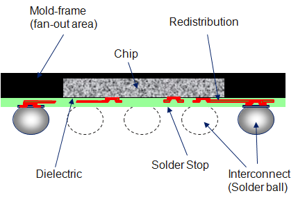
eWLB is a further development of the classical wafer level ball grid array technology (WLB or WLP: wafer level package). The main driving force behind the eWLB technology was to allow fanout and more space for interconnect routing.
All process steps for the generation of the package are performed on the wafer. This allows, in comparison to classical packaging technologies (e. g. ball grid array), the generation of very small and flat packages with excellent electrical and thermal performance at lowest cost. It is common for all WLB technologies, which are built on a silicon wafer, that the interconnects (typically solder balls) fit on the chip (so called fan-in design). Therefore only chips with a restricted number of interconnects can be packaged.
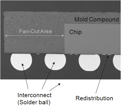
The eWLB technology allows the realization of chips with a high number of interconnects. The package is not created on a silicon wafer as for the classical wafer level package, but on an artificial wafer. Therefore a front-end-processed wafer is diced and the singulated chips are placed on a carrier. The distance between the chips can be chosen freely, but it is typically larger than on the silicon wafer. The gaps and the edges around the chips are now filled with a casting compound to form a wafer. After curing an artificial wafer containing a mold frame around the dies for carrying additional interconnect elements is created. After the build of the artificial wafer (the so-called reconstitution) the electrical connections from the chip pads to the interconnects are made in thin-film technology, as for any other classical wafer level package.
With this technology any number of additional interconnects can be realized on the package in an arbitrary distance (fan-out design). Therefore, this wafer level packaging technology can also be used for space sensitive applications, where the chip area wouldn’t be sufficient to place the required number of interconnects at a suitable distance. The eWLB technology was developed by Infineon, STMicroelectronics and STATS ChipPAC Ltd.[1] First components were brought into market mid of 2009 (mobile phone).
YouTube Encyclopedic
-
1/3Views:56 1876 48210 042
-
Evolution of semiconductor packaging
-
Ball grid array
-
Mod-02 Lec-08 Wafer packaging; Packaging evolution; Chip connection choices
Transcription
[MUSIC] So, this is a topic which has become really interesting in the last ten years or so. So we'll start with some looking at some news, recent flashbacks, right? So this was [COUGH] . Something that we'll try to learn over the course of the next one hour. So, this was a news article in the summer over Wall Street Journal, what it say that that you know, the next iPhone, this was before iPhone five was announced that. It's going to be a millimeter thinner, and a lot of it has to do with the display, and how the packaging of the display is done. This is another news article that says that Xilinx, which is a company that makes [INAUDIBLE]. It has not been able to, you know, get too much performance benefit out of [UNKNOWN] recently. And what they did was they announced these, chips, which are four chips instead of one combined into a single package. And that gives them a much better performance, as compared to. For this one package has four of the [INAUDIBLE] chips and that gives them a much better performance also lower, lowers their costs associated with making that chip. So we learn how is that posssible. Here's another article I used to work with this group at IBM. So it says that IBM is going to announce this working with Micron and they're announcing these 3D chips and it says [INAUDIBLE] card of memory cube. It's right now sampling with with customers right now. And it said that you know, using stacking these chips in a 3D manner. you could you could get significant performance benefits it's good from one of my previous boss at IBM and they presented a paper on this at IBM as well. So these are some of the things we'll try to learn over this week. And this, even more recent, news. So, you know last week there was, some of you might have seen the, the webcast. You know there was an event announcing the iPad Mini. But they also refreshed their, the rest of the product line-up. We'll talk about the display of iPad minis specifically next week when we talk about display. But they, every time they refresh their Mac or iMacs, they have this picture where it shows, you know, the evolution of the Macs from the iMac to you know, the current generation and it Going off it's artistic play on this other picture of, which show evolution of man standing from you know, from ape to the current, you know as we look now, and, you know. A lot of that has to do with packaging and we'll just see over the next over this week. So let's you know, look at evolution of packaging from from 1970s to, to the present date. So I'm sure you know, you must have seen packages which used to look like this right? So this is [UNKNOWN] e lab class in your undergrad, class you'll be using these DIP packages. Which stands for dual inline package. So you'll have. It's called dual inline because there are two of these lines and these pins are in a line. So it's DIP package that that is the first package that was used in the 1970s and still used for you know, hobby electronics and [UNKNOWN] kind of stuff. But there's only so many pins that you can you know, you could have coming out of your package if you have a DIP scheme because You can keep, the only way to have more [UNKNOWN] coming out of this is, you know, you keep making your package taller and taller. But the maximum number of pins that people could get out of this package was around 50 or 60. So this, in 1975 or 80 people introduced quadruple flat package. So instead of having pins coming out on two sides, you will have pins coming out on all four sides. And I'm sure if any of you have done any PCB based soldering, you still use these QFP packages. The common multiple form, sometimes it's called DQFP, sometimes it's called very flat QFP or. So there are multiple variants of this, so there will be typically two or three more letters placed in the front but the last few letters would be QFP. And the maximum amount of pins you can get using these QFP packages well you know, you could have. 50 or 100 of these pins on one side. So you'll have up to 200 or, you know, maximum of 300, 400 pins coming out of this kind of a package. So this was again, you know, not sufficient. People wanted more and more I/Os coming into or out of thier chips. Basically, this was a [INAUDIBLE] leg for your microprocessor chips because microprocessors around this time move from being 16-bit to 32-bit, so you wanted more IO because you essentially moved your the bit crowns on your processors, so they move to this thing called PGA package. Pin grid area packages. And what they were essentially still just having pins on four sides. You could have these gridded array of pins and this is you know If you used to own a PC in 2000. Not 2000 but before that maybe around 95 and 96. Most of these microprocessors you could take them out. You could actually, you know, remove the fan on the top and you could remove this package out because we were using this P, PGA package which you could take out and then place it back again. So it used to be that socket. So there's a male connector and a female connector so you could place it in that female socket and still play around with your microprocessor. [COUGH] So the next evolution of this was, there were some structural soon there were BGA package. You had these pins sticking out and if you tried to increase the density of these pins. they have, you know, these pins have structural limits, and they, every time you take them out, they fall apart. So what people did, again, in 99, was they switched from that PGA package So they switched from an area of from a great area of pins, to a great area of solder bumps. So this is the, it's still the most prevalent package that you, it's used in the industry. And it's essentially a great area of these solder bumps. So you have these solder bumps and What you can see over here, these, is that these solder bumps are just on the periphery of your of your package. They're not in the middle. The reason for this is that the way this package is implemented is you'll have your IC actually placed in the center. So your piece of silicon will be placed in the center. And then you'll be having these gold wires which would be wire bonded to your silicon. And then they'll be wire bonded to your to your to your package. And this package is typically Organic material, it's a laminate, the most common laminate is the FC4 laminate. And, so you'll be having these, wires connecting your die to the actual package. That's why it used to look. Empty, in the middle. The neat thing about it is there are no pins coming out on the side. So if you look, more stuff, we looked at the iPhone 5 tear down at the very beginning of the class. So if you look at that iPhone, PCB from the top. Where you, when your iPad PCB or your Macbook PCB. You won't see any connection on the side. So if you look at this chip right? There's no pins coming out from the side, so it almost looking like the chip is floating in the air. So, you sometimes wonder you know, were the connections are to that chip. So, If you really want to look at those connections, you need to take this board and turn it around by ninety degrees. And then when you look from the side, you see these areas of solder bumps which are connecting your package, which are connecting your chip to this to this PCB. And while it's needed it also makes things very difficult for hobby, hobby electronic people because if now you're a hobby electronic and if one of the chips goes wrong, there's, it's very easy, very hard to you know manually desolder this chip and then solder it back. Especially if it's using this BGA kind of package. So that's, that's, one of the disadvantages but I guess you know not many people open or repair these iPhones themselves so that is the current package which is used. The next evolution which happened around 2000 was instead of. Having those pins just at the periphery. Those having those solder bumps just at the periphery, now you have these solder pods everywhere. So how did that happen now? Where, how is the chip connected? So the next evolution which happened was this flip chip, packaging, and, What really happened was, you used to have that chip connect facing on top. And you'll be having those wire bonds connecting the chip to your package. But now what they did was they took the chip and they flipped it around, so instead of having those wire bonds, you had these all these I/Os coming out from your silicone directly. And then you'll be having these, solder bumps. Which would connect your, connect your piece of silicone to the [UNKNOWN] package directly. And, not all the chips use this. Only chips which have a high, number of, input output pins coming out. they use this flip chip [UNKNOWN] package. So we talked about how so let me you know refresh your memory again. How do we make these micro bumps that you, that enable this flip chip packaging so you, you know this is a process flow of making a microprocessor that we discussed in week two so you'll end up with making all these back end of the line interconnects. And finally what you do is you pattern your very top layer and you expose it, you develop it into that rounded shape. And then you you place some initial metal which acts as a sealer, then you fill it up with the rest, then you electroplate it with copper. And then finally you fill it up. you do electrochemical deposition of solder. So then you take that chip and dip it into a solder bump. And that solder is, it forms the shape of that bump. And there's a lot of technology that goes into how do you detect whether those bumps have holes or not. Because those, if those. If those solderr bumps have air trapped inside them, then that becomes a major cause of failure of your overall package. But, I mean, in the end you, what you do is you strip off that trellis and you're left with a solder bump on top of your chip. And what you do next is I said, we take that chip and just flip it on its head and place it on this package. And that's how most of these microprocessors today are packaged. Another thing which happened a, in around the same time frame, around early 2000 was. this whole movement around doing lead free packaging. So the bill passed, first in Europe, rather [INAUDIBLE] substance built. The same bill was passed in the US and they got, essentially they got rid of lead from the packaging. And if you get rid, rid of, if you get rid of lead from tin solder tin is essentially a very A very soft metal and if you flow current through it it just migrates with the current, so. It forms these things which are called as tin whiskers and especially when you get rid of tin it, you know, it's like a whisker of you know your cat has whiskers. It's similar to that so you are, these tins wires or these tin solders will over the period of time, develop these whiskers which shard your chips over time. So this is, this is one of the disadvantages that you get if you get rid of lead but this is something that people have learned how to live with. But, this is one of the major cause of failure, in one of the pack, in, in in chips that are shipped out in packages without lead. So if you look back and see what drove these changes in the past in chip packaging. They were essentially driven by change in these pin counts. So you know, each of these technology, you look at, multiple technologies they progress and then essentially they saturate and people move to the next paradigm. So people it's, it's, similar thing, you know, with transistors. People started with vacuum tubes, then they. Vaccum tubes stop progressing, they move to BJTs, then they move along BJTs. Then they switch to MOSFETs. And now MOSFETs have stopped progressing. So similar to pack, similar story in packaging, you started with this DIP packages. And then, the number of pins kept on increasing, unless it became too long of a chip, so people moved to this quadraple flat package, that enabled around a maximum of 200 pins. And then people moved to this [INAUDIBLE] package, and that is supposed to allow up to 1,000 pins. And and these, more and more number of I/Os are needed primarily because you're, especially if you are operating a microprocessor. You change it from a 16 bit to a 32 bit to a 64 bit. So that increases your pin count. Nowadays what's driving this pin count is you're moving to more and more system on chip. So if you add more and more functionality to a chip you bring, you need to bring all those I/Os from your other analog chips or from your other from your gyroscope, from your mems chips to your microprocessor. So that's, again adds more and more number of pins that your microprocessor needs to have. So this is a good chart which summarizes all these changes. So from 70 to, you know, 2000, there may be, you know, five, six changes. But where we see now is like there's so many of these changes on the horizon. And we, I'll talk about some of those, but I don't have time to talk about all, but I'll talk about this 2.5D or interposer technology, I'll talk about 3DIC, but there're these so many things going on. There's wafer level packaging there is fan-out packaging. There's. Package on package, so this, it's, it's the same cliche that you heard, technology is changing at a exponential pace and you'll see much more change along the horizon. The driving factor has changed from just being increasing pin count. What's driving this packaging technology now is that you actually get performance benefit. You get power reduction. You get improvement in bandwidth when go to those, go to those packaging technologies. And whenever you hear a term like performance and bandwidth, that means money. So there's. Packaging used to be, you know, maybe 1% of your chip costs. It's moving increasingly to be more than 10, 20% of your chip costs. So there's a lot of money which is Moving in the field of packaging, and that's why everybody wants a piece of the pie, including the company that I work for. So, there are a lot of people who want to get involved in this field right now. [MUSIC]
Process Steps
- Lamination of foil onto carrier (lamination tool)
- Chip placement onto wafer (pick and place tool)
- Molding (mold press)
- De-bonding of carrier (de-bonding tool)
- Flip reconstructed wafer
- Ball drop reflow and wafer test
Advantages
- Low cost (package and test)
- Minimal lateral package size and height
- Excellent electrical and thermal properties
- Number of realizable interconnects on the package is not restricted
- High integration potential for multi-die- and stacked packages
- Upcoming package standard
Disadvantages
- Inspection and repair difficult since visual inspection is restricted
- Mechanical stress between package and board is transmitted stronger than for other package technologies
See also
References
External links
- https://web.archive.org/web/20120305094749/http://www.infineonventures.com/cms/en/corporate/press/news/releases/2007/INFCOM200711-013.html
- http://content.yudu.com/Library/A1mxrk/3DPackagingFebruaryi/resources/4.htm
- https://safe.nrao.edu/wiki/pub/Main/EuropeanMicrowaveWeek08/WFR14-1.pdf
- https://web.archive.org/web/20080517033548/http://www.ciol.com/Semicon/Tech-Watch/News-Reports/Infineon,-ASE-intro-eWLB-package-technology/131107101404/0/
- http://www.statschippac.com/services/packagingservices/waferlevelproducts/~/media/Files/Package%20Datasheets/eWLB.ashx
- http://www.amkor.com/go/packaging/all-packages/cspnl/
- http://www.wsdmag.com/Articles/ArticleID/19576/19576.html
- http://www.semineedle.com/posting/26088?snc=20641&snc=20641[permanent dead link]
- http://ieeexplore.ieee.org/Xplore/login.jsp?url=http%3A%2F%2Fieeexplore.ieee.org%2Fiel5%2F4147209%2F4141004%2F04147210.pdf%3Farnumber%3D4147210&authDecision=-203
- https://web.archive.org/web/20110703111509/http://141.30.122.65/Keynotes/6-Plieninger-ESTC_Keynote_20060907.pdf
- https://web.archive.org/web/20090728202431/http://annualreport2008.infineon.com/de/template.asp?content=innovationen
- Seung Wook Yoon et al. Thermal and Electrical Characterization of eWLB (embedded Wafer Level BGA), Electronic Components and Technology Conference (ECTC), 2010